CMOS
Image Sensors and Camera-on-a-Chip for Low-Light Level Biomedical Applications
Abstract:
With
the advances in deep submicron CMOS technologies, CMOS-based active-pixel
sensors (APS) have become a practical alternative to charge-coupled devices
(CCD) imaging technology. Key advantages of CMOS image sensors are that they
are fabricated in standard CMOS technologies, which allow full integration of
the image sensor along with the analog and digital processing and control
circuits on the same chip and that they are of low cost. Since there is a
practical limit on the minimum pixel size (4~5 μm), then CMOS technology
scaling can allow for an increased number of transistors to be integrated into
the pixel. This truly shows the potential of CMOS technology in imaging
applications, especially for high-speed applications. This work discusses
various active-pixel sensors (APS) and shows the feasibility of using the
DC-level to increase the sensitivity of the pixel for low-level light
applications. Avalanche-photodiodes (APDs) are described, in addition to a
discussion of the breakdown mechanism and micro plasma in avalanche breakdown
for single photon APDs.
Introduction:
Emerging optical
molecular imaging systems have had a revolutionary impact on medicine, bio defense
and environmental testing through techniques such as DNA sequencing, protein
detection, and evaluation of animal models of human cancer. The most sensitive
optical detection system in use is the photomultiplier tube (PMT) but not
preferred as they are costly.
Two alternative
image sensors that can be used for optical molecular imaging systems are
charge-coupled devices (CCDs) and CMOS imagers. CCDs must remain cooled in
order to increase their sensitivity to low-level light for biomedical
applications. Also, CMOS image sensors consume less power, operate at higher
speeds, and offer much higher levels of integration. The advances in deep
submicron CMOS technologies have made CMOS image sensors a practical
alternative to the long dominating CCD imaging technology. One of the main
advantages of CMOS image sensors is that they are fabricated in standard CMOS
technologies, which allow full integration of the image sensor along with the
processing and control circuits on the same chip at a low cost. A CMOS camera-on-chip system leads to
reduction
in power
consumption, cost and sensor size and allows for integration of new sensor
functionalities. Since there is a practical limit on the minimum pixel size
(4~5 μm), then CMOS technology scaling can allow for an increased number of
transistors to be integrated into the pixel. Since digital transistors benefit
more from CMOS scaling properties, digital pixel sensors (DPS) have become very
attractive. A DPS integrates an ADC in each pixel, resulting in massively
parallel readout and conversion that can allow very high speed operation, where
digital data is read out of each pixel. The high speed readout makes CMOS image
sensors suitable for very high-resolution imagers (multi-megapixels)
particularly video applications.
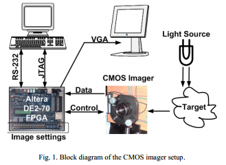
Fig. 1
shows a block diagram of the CMOS imager setup, where the CMOS imager is controlled
by the FPGA board
Different PIXEL
Structures:
Different pixel
structures are used for CMOS imagers. Each pixel structure has its advantages and
is can be suitable for specific applications. In the following sub-sections,
some common CMOS pixel structures are presented, and their applicability to low-light-level
applications are discussed.
1.
Passive-, Active- and Digital-Pixel Sensors
Passive pixel
sensor (PPS) is the earliest and most simple CMOS pixel structure. In PPS, each
pixel consists of a photodiode and a row-select transistor. The PPS has only
one transistor per pixel, and thus it has the highest FF. The active pixel
sensor (APS) is the most popular sensor.
2.
CMOS pixel structure DC Level Mode
APS Active pixel
sensors, in general, have an output with low signal-to-noise ratio (SNR) for
low-levels of light. One way to increase the sensitivity of the APS is to
increase its photodiode’s size. This solution, however, will decrease the
resolution of the imager. Measurement results show that the DC level of the
output can detect light levels which are two decades or less compared to the
swing of the same pixel. For the light power at the low levels of, the SNR of
the DC level stands well above the conventional APS.
3.
Pixels with Avalanche Photodiode
All of the above
pixel structures operate by integrating the photocurrent. In applications where
the signal is changing very fast, short integration times are necessary to
obtain the desired temporal resolution. However, detection of lower levels of
light requires the small photocurrent to be integrated during longer integration
times. These above approaches cannot serve the applications that require sensitivity
and fast response at the same time. A regular p+/n-well diode was fabricated in
standard CMOS technology as a p+ region implanted within an n-well region. In
this diode, the breakdown current will not flow uniformly across the area of
the p+region. The breakdown region of such diode will be at its edge. This is
due to the higher peak electric field caused by the narrower depletion region
at the corners of the diode junction. As the reverse bias increases, the
electric field at the perimeter will reach the onset of avalanche first, and
the current will flow there. However, in APDs, the breakdown region should be
spread over the area of the diode and not at its corners. We have made this
possible by creating a p-type guard ring around the p+ active area of the APD.
To create the guard ring, an n-well region is placed within the p+ region,
which is against the conventional design rules of the standard CMOS. The width
of the guard ring is 3 μm, with a depth of approximately 0.5 μm. It is shown that
the designed device has excellent avalanche characteristics. However, it should
be noted that standard CMOS technology is targeted for digital and analog
applications and not optical imaging devices.
APD Breakdown and Micro
plasma
The proper APD layout
ensures that the maximum electric field happens across the active area of the
APD, rather than at its edges or corners. Impact ionization requires an electric
field of at least E = 300 kV/cm. In a reverse-biased diode, the peak is located
at the metallurgic junction. When the reverse bias is just above the breakdown
voltage, a narrow strip of high electric field region around the metallurgic
junction is where impact ionization occurs, rather than in the entire depletion
region. In this narrow region, any device imperfection can cause a local
disturbance of the electrical field that can lead to a reduction of the
breakdown voltage to a value below the breakdown voltage of the surrounding
uniform junction. These tiny spots will be the site of the localized avalanche
breakdown of the device. This breakdown condition is generally regarded as
being a solid-state analogy of gas discharge plasma, and it is called micro plasma.
The micro plasma can occur at threading dislocations, metal-rich precipitates,
diffusion induced stacking faults, dopant impurity dislocations, diffusion voids
and cracks or mechanical damage. At the onset of avalanching, micro plasmas
switch on and off randomly, producing current pulses of constant height. The
micro plasma is on for an increasing fraction of the time as the voltage
increases until it becomes quiescent. The current carried by micro plasma is
limited by heating, spreading resistance and space charge effects.
CMOS Imager Design
In this
camera-on-a-chip, the row and column scanners are used instead of decoder
circuits in order to
reduce the control
lines coming into the chip. Also, only one input clock is needed to control the
row and column circuitry. The multiplexed output is buffered by an on-chip op-amp,
which provides the chip’s analog output that is only used for testing and comparison
purposes. The analog voltage is routed to the sample-and-hold (S/H) circuit and
ADC. The ADC used is a 6-bit dual-slope integrating topology clocked with a 1 MHz
clock that is provided by the FPGA. A maximum of 64 clock-cycles is required to
complete the conversion, which results in a frame-rate of60 frames/s. The chip
provides both parallel and serial outputs from the ADC for testing purposes.
All elements, including the state-machine, counters and buffers are implemented
on chip. The CMOS imager is tested on an optical table with a 25 mm diameter achromatic
lens that has an effective focal length of 15 mm. The Altera DE2-70 FPGA board is used for
controlling the CMOS imager and all of the FPGA code is written in Verilog. The
tested targets are
kept 44 cm away
from the imager and have a height of about 2 cm.
Conclusion
This paper
demonstrates the great potential of CMOS technology to be used in biomedical
imaging applications. The DC level APS is an excellent choice for low-level
light applications. It uses the same pixel structure as the APS. For
applications that require both sensitivity and fast response, APDs should be
selected. The APDs with active peripheral circuitry offer the highest speed at the
cost of larger pixel sizes. However, by incorporating the advantage of small transistor
sizes of modern CMOS technologies, APDs with peripheral circuitry become an excellent
choice for achieving both high speed and high sensitivity performance. Also,
single photon APD operation is described, including the occurrence of micro plasma
in avalanche breakdown. Micro plasma sites are bi stable below their saturation
currents, and this is the regime where APD can be used. Above the saturation
current level, however, micro plasma is self-sustaining and photoelectron
multiplication is reduced, but the micro plasmas emit light.
Love this valuable information, especially CMOS history. I was searching about CMOS and SiGe technologies to check a fact came online and ended up here, instead going further I read your post and it is helpful. Thanks for sharing your knowledge.
ReplyDeleteAnalog Asic Design & applications